
How Samsung’s Investment in Japan’s Chip Test Line Will Impact the Global Chip Packaging Market
Samsung’s recent investment in a chip test line in Japan is a major development for the global chip packaging market. This move is expected to have a significant impact on the industry, as it will allow Samsung to produce more advanced and reliable chips.
The chip test line in Japan is a state-of-the-art facility that will enable Samsung to test and package chips with greater accuracy and efficiency. This will allow the company to produce chips that are more reliable and cost-effective. Additionally, the test line will enable Samsung to produce chips with higher performance and better power efficiency.
The chip test line will also help Samsung to reduce its production costs. By testing and packaging chips in-house, Samsung will be able to reduce its reliance on third-party chip packaging companies. This will allow the company to save money on production costs, which will ultimately benefit consumers.
The chip test line will also help Samsung to stay ahead of the competition. By producing more reliable and cost-effective chips, Samsung will be able to gain a competitive edge in the global chip packaging market. This will help the company to remain a leader in the industry and ensure its continued success.
Overall, Samsung’s investment in the chip test line in Japan is a major development for the global chip packaging market. This move is expected to have a positive impact on the industry, as it will allow Samsung to produce more reliable and cost-effective chips. This will benefit both the company and consumers alike, as it will help Samsung to remain a leader in the industry and ensure its continued success.
Exploring the Benefits of Samsung’s Advanced Chip Packaging Test Line in Japan
Are you looking for ways to improve the efficiency of your chip packaging process? If so, you should consider investing in Samsung’s advanced chip packaging test line in Japan. This innovative technology offers a range of benefits that can help you streamline your chip packaging process and reduce costs.
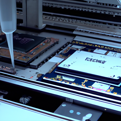
Samsung’s advanced chip packaging test line is designed to provide a comprehensive solution for chip packaging. It features a range of advanced technologies, including a high-speed chip packaging machine, a high-precision chip sorting system, and a high-speed chip testing system. This combination of technologies allows for faster and more accurate chip packaging, resulting in improved efficiency and cost savings.
The high-speed chip packaging machine is capable of packaging chips at speeds of up to 1,000 chips per minute. This allows for faster packaging of chips, resulting in shorter lead times and improved efficiency. The high-precision chip sorting system ensures that chips are accurately sorted and packaged, reducing the risk of errors and improving the quality of the finished product. Finally, the high-speed chip testing system allows for quick and accurate testing of chips, ensuring that only the highest quality chips are used in the packaging process.
In addition to the improved efficiency and cost savings, Samsung’s advanced chip packaging test line also offers a range of other benefits. For example, it is designed to be highly reliable and durable, ensuring that it can withstand the rigors of the chip packaging process. It also features a range of safety features, such as an emergency stop button and a safety guard, to ensure the safety of operators.
Overall, Samsung’s advanced chip packaging test line in Japan offers a range of benefits that can help you streamline your chip packaging process and reduce costs. With its high-speed chip packaging machine, high-precision chip sorting system, and high-speed chip testing system, you can be sure that your chips are accurately packaged and tested, resulting in improved efficiency and cost savings. Investing in this innovative technology can help you take your chip packaging process to the next level.
Analyzing the Impact of Samsung’s Chip Test Line on the Japanese Economy
Samsung’s chip test line has had a significant impact on the Japanese economy. The test line, which was established in Yokkaichi, Japan in 2017, has enabled Samsung to produce more advanced semiconductor chips for its products. This has allowed Samsung to become a major player in the global semiconductor market, and has had a positive effect on the Japanese economy.
The test line has created jobs in the region, providing employment to hundreds of people. This has had a positive effect on the local economy, as the increased employment has led to increased spending in the area. This has resulted in increased economic activity, which has had a positive effect on the local economy.
The test line has also had a positive effect on the Japanese semiconductor industry. The increased production of semiconductor chips has allowed the industry to become more competitive, as Samsung is now able to produce more advanced chips than its competitors. This has allowed the industry to become more competitive on the global market, which has had a positive effect on the Japanese economy.
Finally, the test line has had a positive effect on the Japanese economy by increasing the country’s exports. The increased production of semiconductor chips has allowed Samsung to export more of its products, which has resulted in increased revenue for the country. This has had a positive effect on the Japanese economy, as the increased revenue has allowed the country to invest in other areas of the economy.
Overall, Samsung’s chip test line has had a positive effect on the Japanese economy. The increased employment, increased competitiveness of the semiconductor industry, and increased exports have all had a positive effect on the economy. This has allowed the country to invest in other areas of the economy, which has had a positive effect on the overall economy.
Examining the Challenges of Establishing a Chip Test Line in Japan
Establishing a chip test line in Japan can be a daunting task, but it doesn’t have to be. With the right knowledge and resources, you can make the process much smoother. In this article, we’ll take a look at some of the challenges you may face when setting up a chip test line in Japan and how to overcome them.
One of the biggest challenges you’ll face is the language barrier. Japan has its own unique language and culture, so it’s important to be aware of the differences between English and Japanese. Fortunately, there are many resources available to help you learn the language and understand the culture. Additionally, there are many translation services available to help you communicate with your Japanese partners.
Another challenge you may face is the cost of setting up a chip test line in Japan. The cost of equipment and labor can be quite high, so it’s important to do your research and find the best deals. Additionally, you’ll need to factor in the cost of shipping and taxes.
Finally, you’ll need to consider the regulations and laws in Japan. It’s important to understand the laws and regulations that apply to chip testing in Japan, as well as any other relevant laws. Additionally, you’ll need to make sure that your chip test line meets all safety and quality standards.
Establishing a chip test line in Japan can be a challenging process, but with the right knowledge and resources, you can make it much easier. By understanding the language, researching the costs, and familiarizing yourself with the laws and regulations, you can ensure that your chip test line is successful.
Exploring the Potential of Samsung’s Chip Test Line in Japan for Advanced Chip Packaging
Welcome to the exciting world of advanced chip packaging! Samsung’s chip test line in Japan is a great place to explore the potential of this technology.
Advanced chip packaging is a process that involves the integration of multiple components into a single package. This technology has the potential to revolutionize the way we use and interact with electronics. By combining multiple components into a single package, it can reduce the size and weight of electronic devices, while also increasing their performance and reliability.
At Samsung’s chip test line in Japan, you can explore the potential of advanced chip packaging. The test line is equipped with the latest technology and equipment, allowing you to test and evaluate the performance of different chip packages. You can also use the test line to develop new chip packages and explore new applications for them.
The test line is also a great place to learn more about advanced chip packaging. Samsung’s experts are available to provide guidance and advice on the best way to use the technology. They can also help you understand the different types of chip packages and how they can be used in different applications.
Finally, the test line is a great place to network with other professionals in the field. You can meet and collaborate with other experts in the industry, and learn more about the latest developments in advanced chip packaging.
We hope you enjoy exploring the potential of advanced chip packaging at Samsung’s chip test line in Japan. With the right guidance and support, you can unlock the potential of this technology and create amazing new products and applications.